Back illuminated 16 channel photodiode array
17 Feb 2015
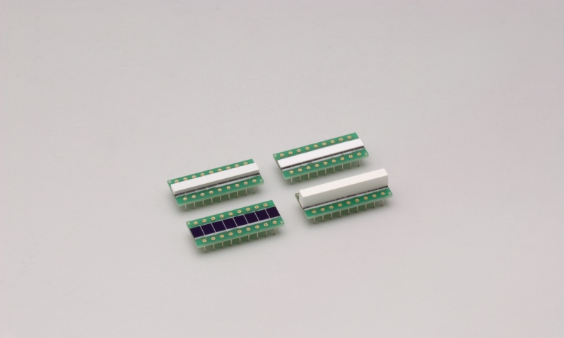
Hamamatsu Photonics has launched a back illuminated 16 channel photodiode array (PDA), designed for use in X-ray non-destructive testing applications.
The S11299 uses flip-chip technology that allows the PDA to receive scintillation light from the back side of the array.
This flip-chip approach reduces the need for gold bond wires and junction layers on the light input side, reducing the risk of wire bond damage during scintillator mounting.
The S11299 uses a slender board design, with a vertical height of just 10.2mm. This allows for long and narrow arrays to be constructed.
Additionally, the S11299 is suitable for dual energy imaging, by combining two arrays with differing scintillator thickness in a vertical structure. The existing S11212 series is ideal for this and various configurations can be designed to match any application requirement.
For more information, please contact: +44 (0)1707 294 888, E: info@hamamatsu.co.uk or visit: www.hamamatsu.com
